Post by Shadyreaper on Nov 1, 2016 9:07:03 GMT -5
I have not done these mods myself they were taken for the K|ngp|n cooling Forums these mods were done by TiN and this is his guide and original link to post forum.kingpincooling.com/showthread.php?p=31301#post31301
[/COLOR]
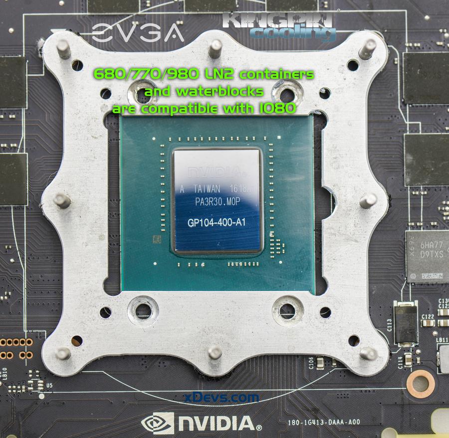
No need worry about this topic as mount hole locations and clearance is exactly same as older 680/780/780Ti/980/980Ti reference cards. Previous generation GPU coolers will fit GTX 1080 just fine.
New Pascal processors also have no metal shim around the core anymore, so be extra careful mounting your cooling solution and keep surfaces parallel. Cracked GPU silicon never did any good to card’s functionality.
Best to have full 8-points brackets to ensure good and even mount pressure across all GPU sides. It’s compatible with all TEK9 FAT and TEK9 SLIM containers and can be bought separately on Kingpincooling.com shop.
STEP 1 – Prep your bench[/COLOR]
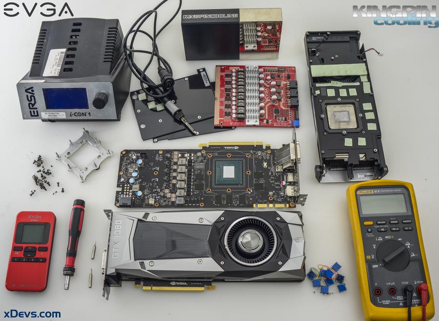
Few common tools for modding GTX 1080 card are required. Likely you already have them, if you reading this guide. GTX 1070 PCB can follow same idea, but this time you will have to find exact way by youself. I’ll focus solely on GTX 1080 in this guide, targeting overclockers and enthusiasts.
* EVGA GEFORCE GTX 1080 FE (I my case - 08G-P4-6180-KR) card to play with.
* 2pcs 1 KΩ multi-turn VRs (trim pots).
* 1pcs 1 MΩ multi-turn VR (trim pot).
* 1pcs 100 KΩ multi-turn VR (trim pot).
* 3pcs 10 Ω 0805 size resistors (example here in Digikey)
* 20-50W soldering iron for mods, 80-120W for EPOWER mod.
* Spool of generic 28-32AWG insulated wire
* Soldering FLUX
* Kingpincooling TEK9 FAT
* DMM (I use good handheld Fluke 87V and high-performance bench Keithley 2002, but actually any 10$ DMM can fit needs of this guide)
* Low-ESR capacitors (2.5 or 4V rated, 680-820uF , etc) if you like to juice things up, but not required.
I use ERSA iCON-1 soldering station to perform all below mods. ERSA 102CDLF2.4 tip covered all trimpot mods for this guide, with tip temperature set to 290 °C. Before starting with soldering, make sure usual mess on table cleaned, with all the things you don't need out.
Good lights are mandatory to better see those tiny components and points on PCB.
I often check joints with stereo microscope like this one, but even simple magnifying glass will help. Time to start:
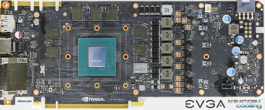
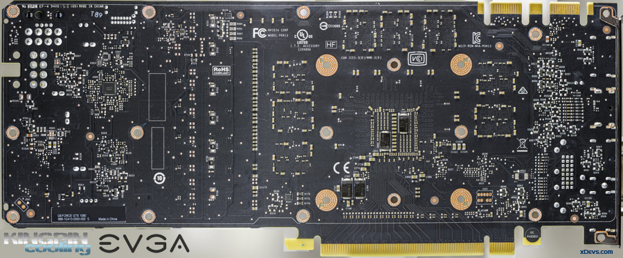
Two high-resolution 105 megapixel photo will surely help you to study a bit location of all key components on GTX 1080 reference board. :whistle:
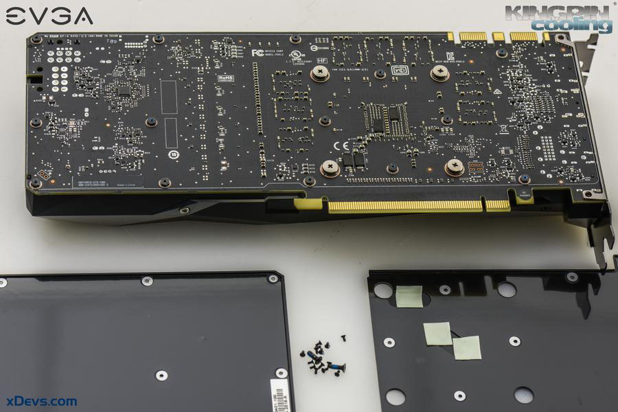
Rear bottom side:
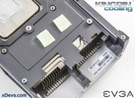
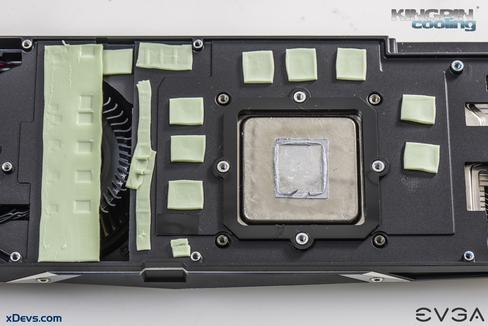
Also quick look on heatsink, which using thermal chamber:
Unlike many of custom AIB coolers, this one pushing all the hot air outside of the chassis, so it's way better for small/tightly packed chassis. Everything else is similar to previous generation cards with radial fan and finned aluminum heatsink.
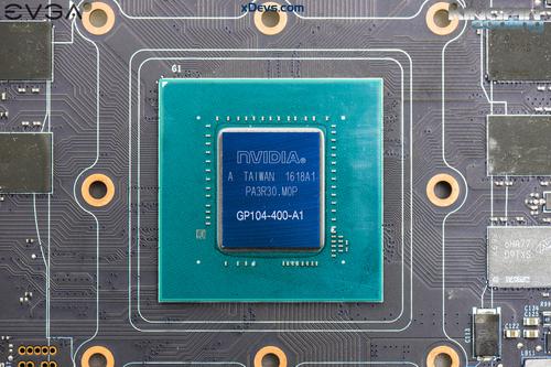
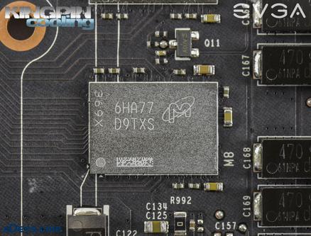
And final close-up of GPU package and used Micron GDDR5X memory:
GPU bears GP104-400-A1 marking, meaning it's mid-range 104 core (GTX 680 was GK104, GTX 980 was GM204, while Titan/Ti cores are GK100/GM200), silicon revision A1. Silicon manufactured by TSMC, with date code week 18 of 2016. Few more things we can learn also from the memory IC datasheet, such as nominal voltage reduced from 1.55V (GDDR5) to 1.35V and extra voltage rail VPP was added, at 1.8V level. GTX 1070 using usual GDDR5.
STEP 2 – Strip the card[/COLOR]
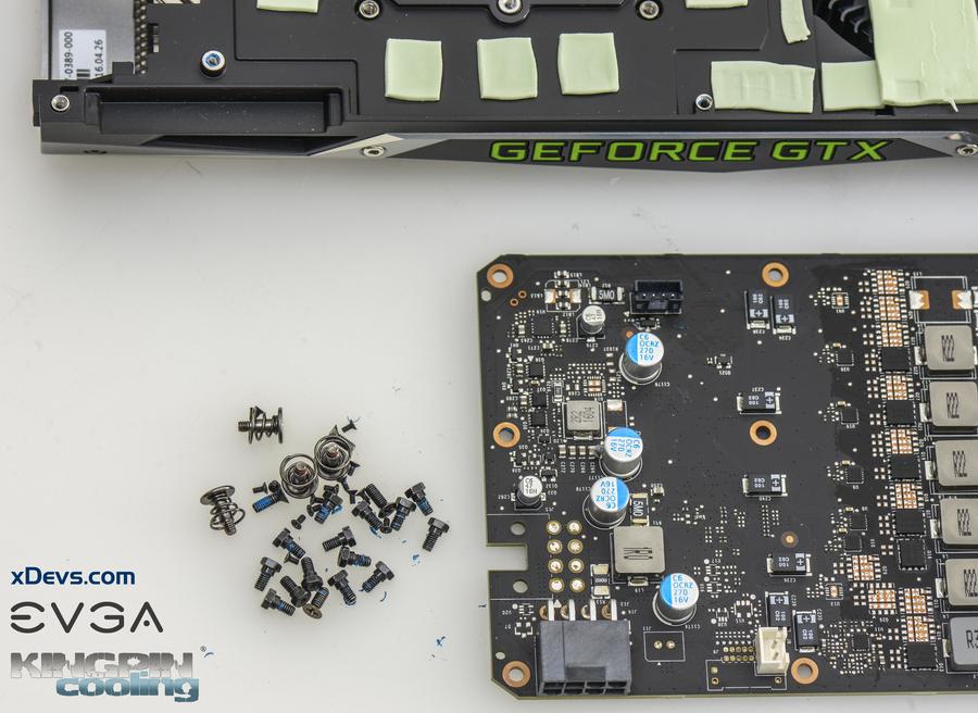
Cooler must be removed from the card to get access of both PCB sides. You will need hexagon driver to remove nut-head screws which used to hold backplate and PCB together.
Keep all those fancy custom screws safe, so you can put heatsink back after you done, if you wish to revert card to normal air use afterwards.
Now we have easy access to components for measurements and modifications. I’ll skip on boring part of measuring various points, so we can jump right into good stuff, starting with removing power limitations.
STEP 3 – Uncorking your power[/COLOR]
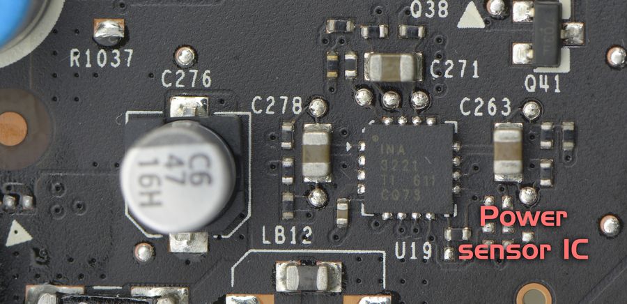
Good old friend, Texas Instruments INA3221 power sensor IC is used again. This chip used to measure voltage, current and power on +12VDC input rails using external current shunts.
Current shunt is special type of resistor, to generate voltage drop which closely depends on amount of current flowing thru it. This drop measured, and having resistance known, current and power can be easily calculated.
This way NV driver can detect real-time power consumption and adjust GPU’s clock speed and performance automatically to keep power within specified levels. If power go over that limit - your performance/clocks will be reduced automatically. We don't want this to happen, so one way is to tamper circuit to report lower power. It sounds more difficult than it actually is, so here are two photos to illustrate the mod:
Current shunts can be found on PCB, with marks RS1, RS2, RS3 on PCB. Shunts usually have R002 or R005 or 2M0/5M0 mark on top. Sometimes there are no marks, but look is always very similar. These shunts are located close to input power connectors, as all copper power going the main VRM circuitry need to go thru these shunts.
So if we reduce reported current by adding parallel 10Ω resistors to marked 0805 caps on photo below.
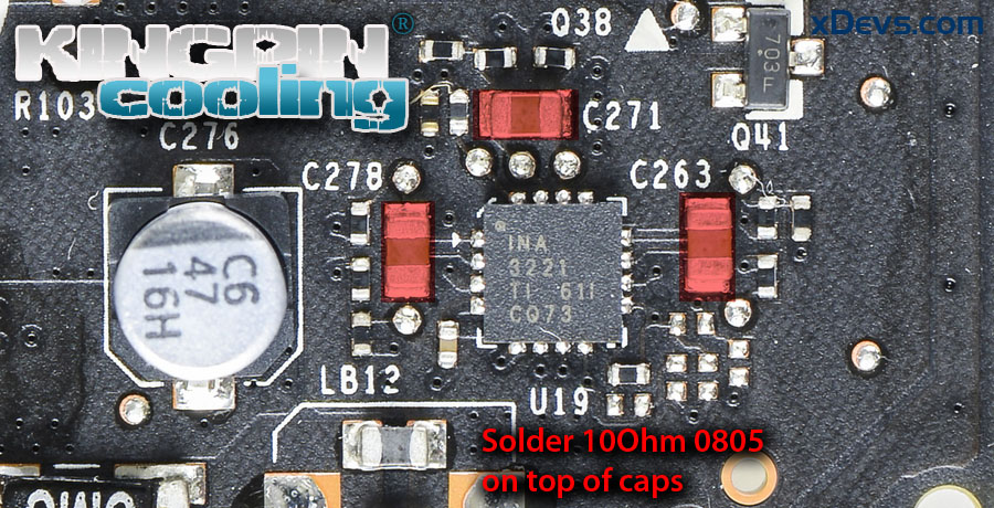
This is very similar to other NV cards, and bit more details was already covered here and here. Check those guides to refresh memory.
STEP 4 – GPU Voltage mod[/COLOR]
First modification is one to adjust GPU core voltage. This is most popular one by far, and often (but not always, just like in case of Maxwell!) extra voltage can help to get better stability and higher clocks, given no other limitations are hit. Maximum available voltage thru software only control on reference cards are very limited, usually around 1.2V, so that's why hardware mod is required to get over this limit.
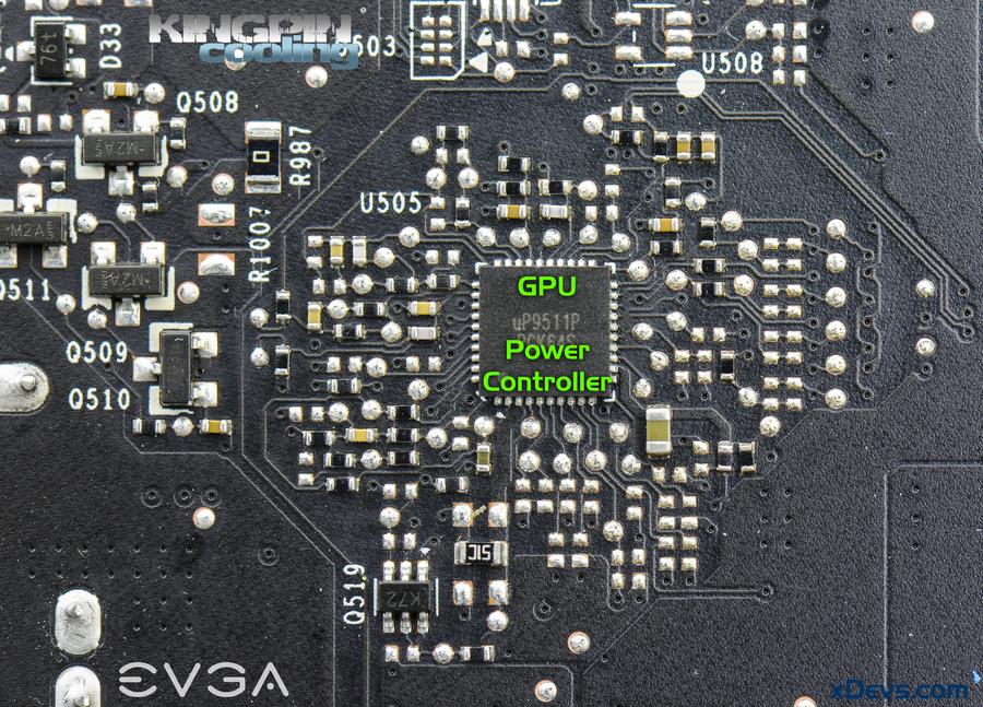
GPU power controller, which is now new UPI uP9511P, instead of ON NCP81174 which was used on previous reference GTX 980 and GTX 980 Ti cards. UPI’s site is way obsolete and lacks of any useful information, so I could only guess from layout and probing around that this controller supports at least 6 phases, has no digital interface or parallel VID code setting (no array of 6-8 resistors found around to set VID voltage code) and unlikely to have digital interface like I2C.
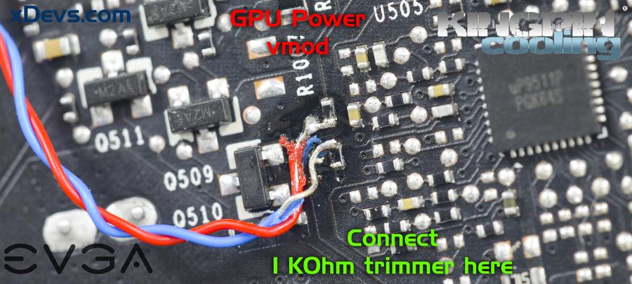
But no worries, by tracing where GPU power signals come around chip voltage sense lines were quickly found. These are two lines from resistors near R1007 and Q510 location. Enough to know for us to do the voltage mod! :cool:
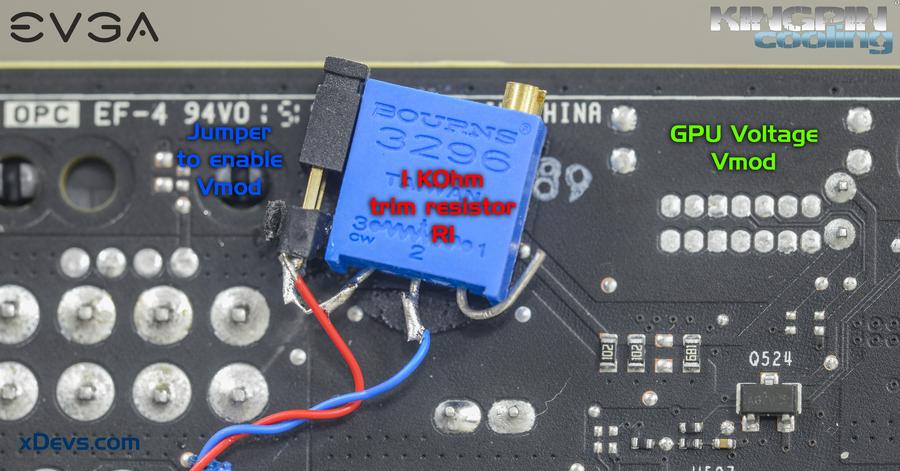
Prepare VR’s, in this case one 1 KΩ nominal resistance multiturn variable resistor (potentiometers). I like to use very common blue square 3296 type. There are many electronic components retailers have these available for sale, and it should be easy to find suitable resistors from your local store.
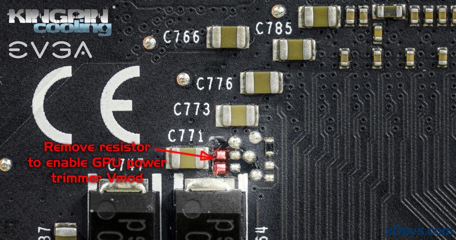
Now remove resistor marked in red box on photo below to enable adjustment on feedback sense.
Without this step voltage will be directed by GPU to VRM connection, and modification would not work as expected.
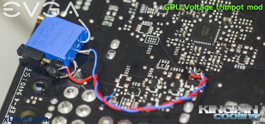
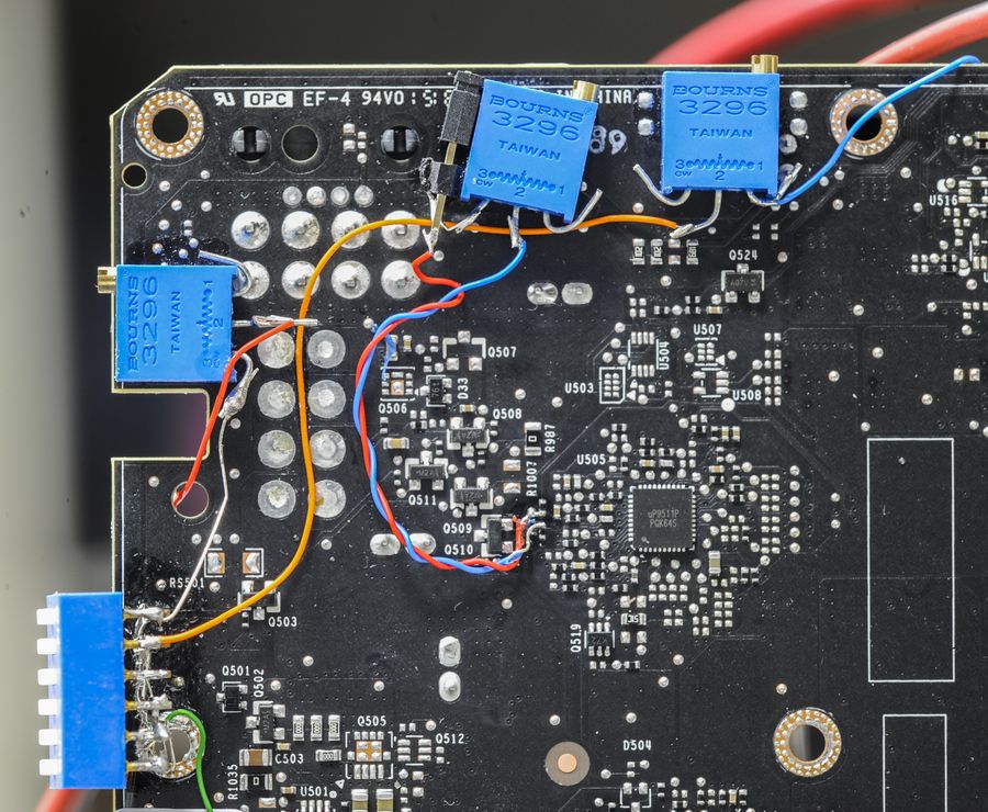
Fix 1 KΩ trimmer at PCB, similar to photo below. This is to ensure it does not rip off or short anything later on when you adjust it with screwdriver. Easy 2-position jumper pin header used also to allow disabling mod on the fly. That could be useful for checking if any issue with overvoltage. Two AWG32 wires or similar needed to connect trimmer to specific points.
Before you solder everything down, set and measure resistor at maximum value (resistance measured by DMM across both wires, not connected to anything), which should be around 1000 Ω. Not such a great idea to boot card right at 1.9V :rolleyes: . Solder wires to tiny spots near GPU voltage controller.
Order of wire connections here is not important, as resistor is bidirectional element. Just make sure your connection is to same points as on the photo, and that should do it. Overall mod can be checked with final photo.
Since traces and solder points on PCB are thin and easy to peel off, make sure you fix wires to the PCB in few places, so it does not move so easily. Few drops of cyanoacrylate superglue drops on areas free from components will do job well.
You can go over 1.6+V with this kind of modification easily, so it’s also can be suitable for extreme overclocking. But beware, safe voltages even on LN2 are rather around 1.3-1.5ish range, as this 5-phase VRM is not exactly designed for high-power/high-voltage use. And noone will tell you what is best or optimal voltage for your specific GPU sample on your card, so it's all the homework to find best spot thru testing various clocks/voltages.
Note that GPU resistance on GP104 is very low, opposite to many previous GPU generations. I measured it around 90-120 mΩ (0.09-0.12 Ohm) using four-wire resistance measurement with expensive high-accuracy Keithley Model 2002 DMM.
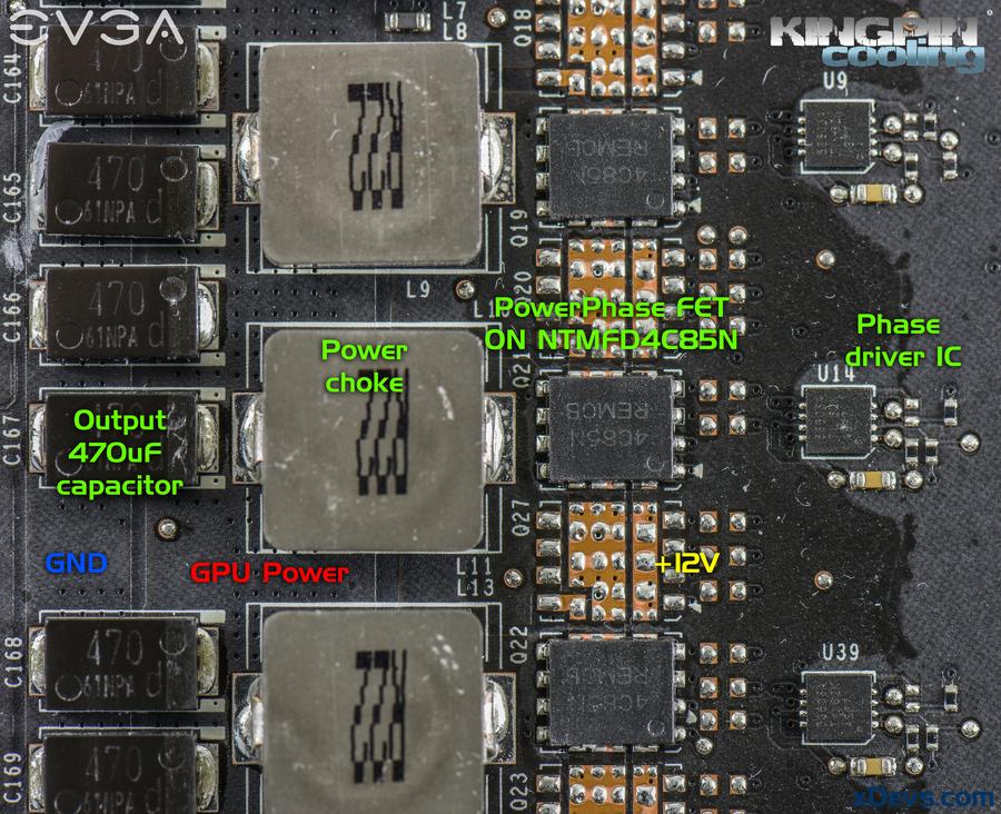
If you plan to use waterblock or Kingpincooling TEK9 LN2 container as GPU cooler, make sure you have good 120mm fan over VRM area to ensure good airflow and acceptable temperatures (best under 70°C) when overclocking. Each phase for GPU power is capable of providing ~25A of current. Power switching is done by ON Semiconductor NTMFD4C85N PowerPhase Dual NFETs in compact SO8FL package.
Reference design PCB have six phases originally for GPU power with dual PowerPhase arrays on each phase, but currently only 5 phases are used for the GTX 1080 with only one PowerPhase Dual NFET per phase. This is done to bring manufacturing cost down and keep better efficiency on low/medium loads, rather than going all out for max power capacity. It’s common design compromise, as higher power regulators are also wasting bit more power in parasitic losses when actual power consumption not pushed to those higher limits. :nowr:
STEP 5 – Memory voltage trim-pot mod[/COLOR]
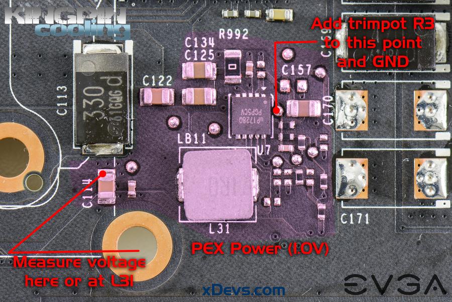
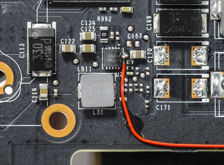
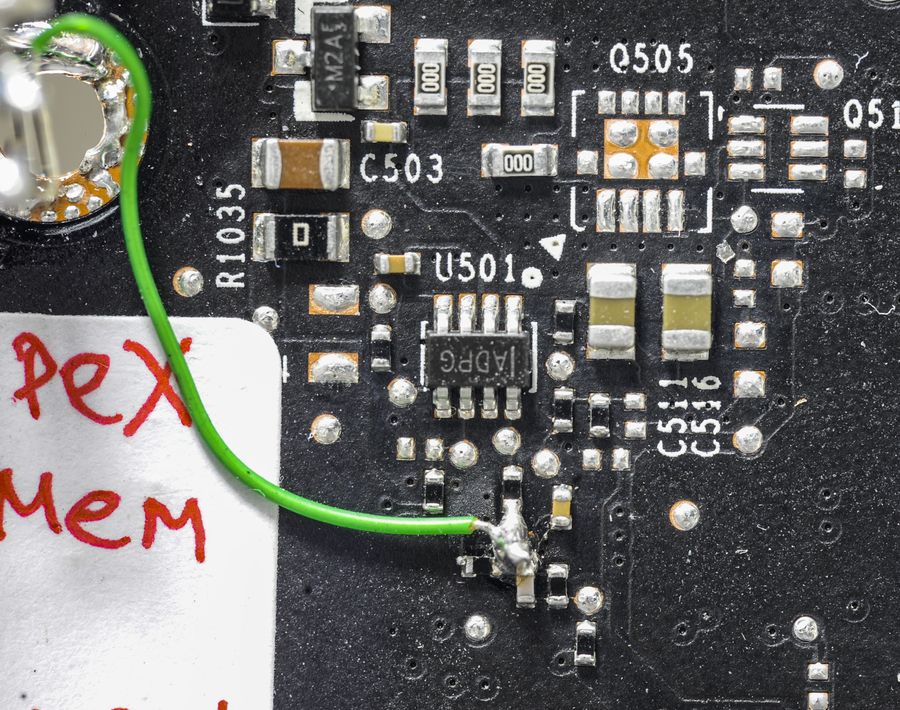
Memory VRM using only one phase, with same 25A PowerPhase dual NFET and output 1.35V for GDDR5X memory chips.
To raise voltage all you need to do is just 1KΩ trimmer to GND at marked point on photo.
STEP 6 – PLL Voltage trim-pot mod[/COLOR]
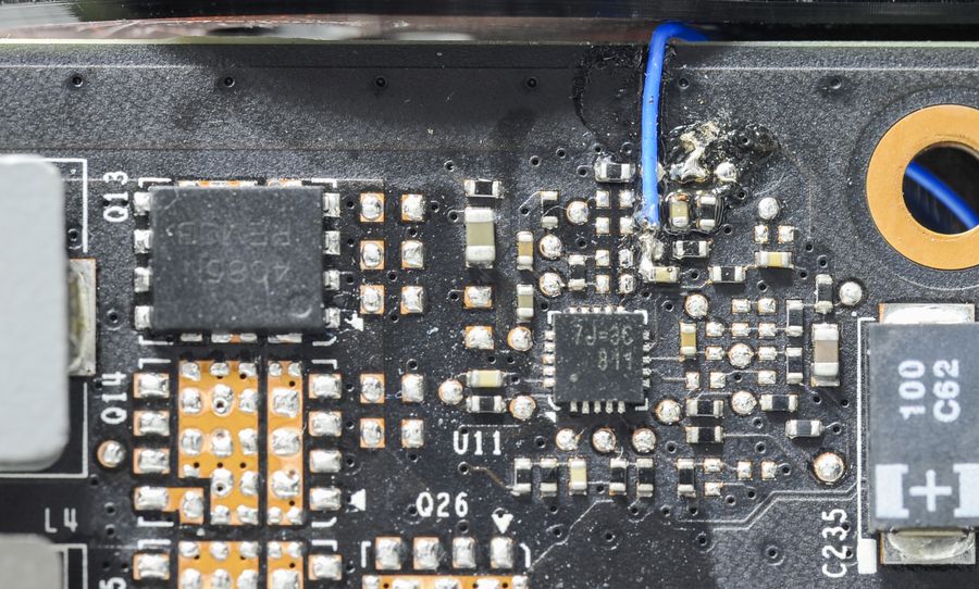
PLL regulator is common and well known from previous GPUs, so nothing new here. PWM chip used is uPI UP1628Q in tiny DFN package. Modification to raise voltage on it is straight forward and involve connection of 100KΩ trimmer to GND and point on the photo above.
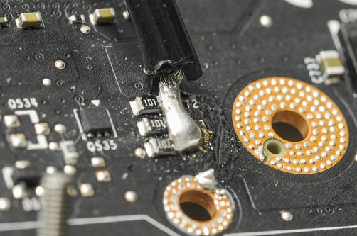
Monitoring of PLL voltage output can be done by soldering wire to location of three resistors near bottom left GPU fan-sink mount hole.
STEP 7 – AUX Voltage trim-pot mod[/COLOR]
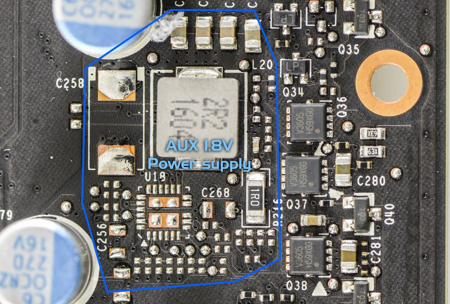
Since GDDR5X memory now need extra voltage, there is additional 1.8V power supply on the card, right near power monitoring circuits.
High-value 1MΩ trimmer is required for this mod. Be careful, as too low resistance which causes higher than 2V output may destroy card easily. Resistor trim point to GND is shown below:
This mod unlikely to help overclocking, so it’s up to you if it’s worth having a risk.
Now you all set for some serious testing.
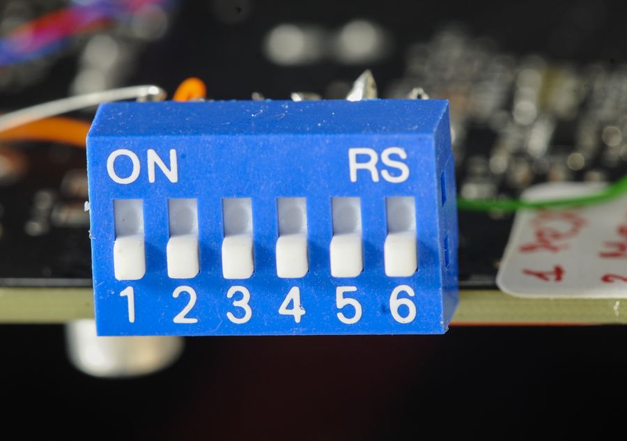
I also used DIP switch to get ability of turning off memory and PLL vmods ON/OFF in real-time.
Other useful tricks and quirks for Pascal[/COLOR]
Earliest driver which supports 1080 is 368.22 Beta which needs nv_disp.inf modification (just replace ID from 980Ti to 1080's one 1B80). This will require disabling driver signing thru advanced reboot on Windows.
Eary official driver for 1080 is 368.25.
STEP X – BONUS[/COLOR]
Well...for that you go to extended and latest version of this guide always available at xDevs.com.
If you want to reuse photos or data from this guide, make sure you mention links and original source here. Just to be nice and keep community friendly, you know.
Stay tuned and let us know your Pascal overclocking uncorkment experience. :up:
This guide is evolution of my usual “uncork series”. If you have no idea what that mean, read previous ones:
Reference GTX 680 – Uncorking KEPLER
GTX 680 Classified – Uncorking guide
Reference GTX 780/780Ti – Big KEPLER
EVGA GTX 980 Ti K|NGP|N OC Guide
Uncorking EVGA GeForce GTX 980 for overclocking
Removing power limits on any NV card
Using Raspberry Pi to control your VGA VRM
Here we check out reference EVGA GeForce GTX 1080, also known as “Founders Edition”.
No doubt, modifying your GFX to for these kind of results require bit of above-minimal soldering skill knowledge and cold mind. I’ll skip on obvious things, like probing voltage/resistance with multimeter, what is trimpot and how to solder, as these things were explained before in previous guides, linked above.
As usual, you are on your own when doing even little simple mod. If you card burns in flames or just simply stop working, please, do not try to RMA it or expect a support from manufacturers. Anything below this paragraph in this article is NOT covered by any kind of warranty, and provided AS IS only, without any support from EVGA or NVIDIA. You are on your own here, so "yes, don’t try this at home" very apply here. Any RMA attempt of soldered card is easily diagnosed and will be rejected.
Cooling compatibility
No need worry about this topic as mount hole locations and clearance is exactly same as older 680/780/780Ti/980/980Ti reference cards. Previous generation GPU coolers will fit GTX 1080 just fine.
New Pascal processors also have no metal shim around the core anymore, so be extra careful mounting your cooling solution and keep surfaces parallel. Cracked GPU silicon never did any good to card’s functionality.
Best to have full 8-points brackets to ensure good and even mount pressure across all GPU sides. It’s compatible with all TEK9 FAT and TEK9 SLIM containers and can be bought separately on Kingpincooling.com shop.
STEP 1 – Prep your bench[/COLOR]
Few common tools for modding GTX 1080 card are required. Likely you already have them, if you reading this guide. GTX 1070 PCB can follow same idea, but this time you will have to find exact way by youself. I’ll focus solely on GTX 1080 in this guide, targeting overclockers and enthusiasts.
* EVGA GEFORCE GTX 1080 FE (I my case - 08G-P4-6180-KR) card to play with.
* 2pcs 1 KΩ multi-turn VRs (trim pots).
* 1pcs 1 MΩ multi-turn VR (trim pot).
* 1pcs 100 KΩ multi-turn VR (trim pot).
* 3pcs 10 Ω 0805 size resistors (example here in Digikey)
* 20-50W soldering iron for mods, 80-120W for EPOWER mod.
* Spool of generic 28-32AWG insulated wire
* Soldering FLUX
* Kingpincooling TEK9 FAT
* DMM (I use good handheld Fluke 87V and high-performance bench Keithley 2002, but actually any 10$ DMM can fit needs of this guide)
* Low-ESR capacitors (2.5 or 4V rated, 680-820uF , etc) if you like to juice things up, but not required.
I use ERSA iCON-1 soldering station to perform all below mods. ERSA 102CDLF2.4 tip covered all trimpot mods for this guide, with tip temperature set to 290 °C. Before starting with soldering, make sure usual mess on table cleaned, with all the things you don't need out.
Good lights are mandatory to better see those tiny components and points on PCB.
I often check joints with stereo microscope like this one, but even simple magnifying glass will help. Time to start:
Two high-resolution 105 megapixel photo will surely help you to study a bit location of all key components on GTX 1080 reference board. :whistle:
Rear bottom side:
Also quick look on heatsink, which using thermal chamber:
Unlike many of custom AIB coolers, this one pushing all the hot air outside of the chassis, so it's way better for small/tightly packed chassis. Everything else is similar to previous generation cards with radial fan and finned aluminum heatsink.
And final close-up of GPU package and used Micron GDDR5X memory:
GPU bears GP104-400-A1 marking, meaning it's mid-range 104 core (GTX 680 was GK104, GTX 980 was GM204, while Titan/Ti cores are GK100/GM200), silicon revision A1. Silicon manufactured by TSMC, with date code week 18 of 2016. Few more things we can learn also from the memory IC datasheet, such as nominal voltage reduced from 1.55V (GDDR5) to 1.35V and extra voltage rail VPP was added, at 1.8V level. GTX 1070 using usual GDDR5.
STEP 2 – Strip the card[/COLOR]
Cooler must be removed from the card to get access of both PCB sides. You will need hexagon driver to remove nut-head screws which used to hold backplate and PCB together.
Keep all those fancy custom screws safe, so you can put heatsink back after you done, if you wish to revert card to normal air use afterwards.
Now we have easy access to components for measurements and modifications. I’ll skip on boring part of measuring various points, so we can jump right into good stuff, starting with removing power limitations.
STEP 3 – Uncorking your power[/COLOR]
Good old friend, Texas Instruments INA3221 power sensor IC is used again. This chip used to measure voltage, current and power on +12VDC input rails using external current shunts.
Current shunt is special type of resistor, to generate voltage drop which closely depends on amount of current flowing thru it. This drop measured, and having resistance known, current and power can be easily calculated.
This way NV driver can detect real-time power consumption and adjust GPU’s clock speed and performance automatically to keep power within specified levels. If power go over that limit - your performance/clocks will be reduced automatically. We don't want this to happen, so one way is to tamper circuit to report lower power. It sounds more difficult than it actually is, so here are two photos to illustrate the mod:
Current shunts can be found on PCB, with marks RS1, RS2, RS3 on PCB. Shunts usually have R002 or R005 or 2M0/5M0 mark on top. Sometimes there are no marks, but look is always very similar. These shunts are located close to input power connectors, as all copper power going the main VRM circuitry need to go thru these shunts.
So if we reduce reported current by adding parallel 10Ω resistors to marked 0805 caps on photo below.

This is very similar to other NV cards, and bit more details was already covered here and here. Check those guides to refresh memory.
STEP 4 – GPU Voltage mod[/COLOR]
First modification is one to adjust GPU core voltage. This is most popular one by far, and often (but not always, just like in case of Maxwell!) extra voltage can help to get better stability and higher clocks, given no other limitations are hit. Maximum available voltage thru software only control on reference cards are very limited, usually around 1.2V, so that's why hardware mod is required to get over this limit.
GPU power controller, which is now new UPI uP9511P, instead of ON NCP81174 which was used on previous reference GTX 980 and GTX 980 Ti cards. UPI’s site is way obsolete and lacks of any useful information, so I could only guess from layout and probing around that this controller supports at least 6 phases, has no digital interface or parallel VID code setting (no array of 6-8 resistors found around to set VID voltage code) and unlikely to have digital interface like I2C.
But no worries, by tracing where GPU power signals come around chip voltage sense lines were quickly found. These are two lines from resistors near R1007 and Q510 location. Enough to know for us to do the voltage mod! :cool:
Prepare VR’s, in this case one 1 KΩ nominal resistance multiturn variable resistor (potentiometers). I like to use very common blue square 3296 type. There are many electronic components retailers have these available for sale, and it should be easy to find suitable resistors from your local store.
Now remove resistor marked in red box on photo below to enable adjustment on feedback sense.
Without this step voltage will be directed by GPU to VRM connection, and modification would not work as expected.
Fix 1 KΩ trimmer at PCB, similar to photo below. This is to ensure it does not rip off or short anything later on when you adjust it with screwdriver. Easy 2-position jumper pin header used also to allow disabling mod on the fly. That could be useful for checking if any issue with overvoltage. Two AWG32 wires or similar needed to connect trimmer to specific points.
Before you solder everything down, set and measure resistor at maximum value (resistance measured by DMM across both wires, not connected to anything), which should be around 1000 Ω. Not such a great idea to boot card right at 1.9V :rolleyes: . Solder wires to tiny spots near GPU voltage controller.
Order of wire connections here is not important, as resistor is bidirectional element. Just make sure your connection is to same points as on the photo, and that should do it. Overall mod can be checked with final photo.
Since traces and solder points on PCB are thin and easy to peel off, make sure you fix wires to the PCB in few places, so it does not move so easily. Few drops of cyanoacrylate superglue drops on areas free from components will do job well.
You can go over 1.6+V with this kind of modification easily, so it’s also can be suitable for extreme overclocking. But beware, safe voltages even on LN2 are rather around 1.3-1.5ish range, as this 5-phase VRM is not exactly designed for high-power/high-voltage use. And noone will tell you what is best or optimal voltage for your specific GPU sample on your card, so it's all the homework to find best spot thru testing various clocks/voltages.

Note that GPU resistance on GP104 is very low, opposite to many previous GPU generations. I measured it around 90-120 mΩ (0.09-0.12 Ohm) using four-wire resistance measurement with expensive high-accuracy Keithley Model 2002 DMM.
If you plan to use waterblock or Kingpincooling TEK9 LN2 container as GPU cooler, make sure you have good 120mm fan over VRM area to ensure good airflow and acceptable temperatures (best under 70°C) when overclocking. Each phase for GPU power is capable of providing ~25A of current. Power switching is done by ON Semiconductor NTMFD4C85N PowerPhase Dual NFETs in compact SO8FL package.
Reference design PCB have six phases originally for GPU power with dual PowerPhase arrays on each phase, but currently only 5 phases are used for the GTX 1080 with only one PowerPhase Dual NFET per phase. This is done to bring manufacturing cost down and keep better efficiency on low/medium loads, rather than going all out for max power capacity. It’s common design compromise, as higher power regulators are also wasting bit more power in parasitic losses when actual power consumption not pushed to those higher limits. :nowr:
STEP 5 – Memory voltage trim-pot mod[/COLOR]
Memory VRM using only one phase, with same 25A PowerPhase dual NFET and output 1.35V for GDDR5X memory chips.
To raise voltage all you need to do is just 1KΩ trimmer to GND at marked point on photo.
STEP 6 – PLL Voltage trim-pot mod[/COLOR]
PLL regulator is common and well known from previous GPUs, so nothing new here. PWM chip used is uPI UP1628Q in tiny DFN package. Modification to raise voltage on it is straight forward and involve connection of 100KΩ trimmer to GND and point on the photo above.
Monitoring of PLL voltage output can be done by soldering wire to location of three resistors near bottom left GPU fan-sink mount hole.
STEP 7 – AUX Voltage trim-pot mod[/COLOR]
Since GDDR5X memory now need extra voltage, there is additional 1.8V power supply on the card, right near power monitoring circuits.
High-value 1MΩ trimmer is required for this mod. Be careful, as too low resistance which causes higher than 2V output may destroy card easily. Resistor trim point to GND is shown below:
This mod unlikely to help overclocking, so it’s up to you if it’s worth having a risk.
Now you all set for some serious testing.
I also used DIP switch to get ability of turning off memory and PLL vmods ON/OFF in real-time.
Other useful tricks and quirks for Pascal[/COLOR]
Earliest driver which supports 1080 is 368.22 Beta which needs nv_disp.inf modification (just replace ID from 980Ti to 1080's one 1B80). This will require disabling driver signing thru advanced reboot on Windows.
Eary official driver for 1080 is 368.25.
STEP X – BONUS[/COLOR]
Well...for that you go to extended and latest version of this guide always available at xDevs.com.
If you want to reuse photos or data from this guide, make sure you mention links and original source here. Just to be nice and keep community friendly, you know.
Stay tuned and let us know your Pascal overclocking uncorkment experience. :up:
